


Том 18, № 6 (2025)
- Год: 2025
- Статей: 7
- URL: https://journals.eco-vector.com/1993-8578/issue/view/14061
- DOI: https://doi.org/10.22184/1993-8578.2025.18.6

Нанотехнологии
Исследование микроразмерных поверхностных деформаций на основании анализа данных атомно-силовой микроскопии методом цифровой корреляции изображений
Аннотация
Показана применимость метода цифровой корреляции изображений (ЦКИ) к топографиям атомно-силовой микроскопии (АСМ) при локальной нагрузке. Исследован технически чистый титан Grade 4 после равноканального углового прессования по схеме Конформ. Локальная деформация формировалась микросферическим алмазным индентором (R = 2,5 мкм). АСМ-сканирование области до/после вдавливания выполнялось с регистрацией по квадратному шаблону царапин (~1 мкм). Предобработка включала подавление артефактов и выравнивание поля. Субпиксельная ЦКИ по локальным окнам обеспечила восстановление радиальной и тангенциальной компонент поля смещений. Получены непрерывные карты, фиксирующие распространение возмущений за пределы контактной зоны и особенности локальной пластической деформации. Результаты подтверждают техническую реализуемость и информативность ЦКИ для количественного картирования смещений при наноиндентировании ультрамелкозернистого титана.
 326-334


Исследование морфологии коронавируса с помощью атомно-силовой микроскопии
Аннотация
Атомно-силовая микроскопия позволяет с высоким разрешением визуализировать оболочечные вирусы, к которым относятся вирусы семейства Coronaviridae, исследовать характер их адсорбции на различных поверхностях, измерять механические свойства вирусов, оценивать влияние изменения среды, температуры на морфологию. С помощью силовых кривых можно посчитать модуль Юнга вирусной частицы, оценить характер взаимодействия между белком оболочки и клеточным рецептором, даже померить силу этого взаимодействия. Все эти возможности не только позволяют характеризовать вирусы, но и помогают предотвращать распространение болезнетворных патогенов в человеческой популяции и выбирать оптимальную стратегию лечения.
336-344
О размере атома
Аннотация
В современной метрологии размер атома определяется статистически как половина межатомного расстояния в кристаллической решетке, а не через прямое измерение изолированного атома. Сканирующая туннельная микроскопия (СТМ) и атомно-силовая микроскопия (АСМ) – ключевые инструменты для прямого наблюдения и измерения геометрии отдельных атомов, слабо связанных с подложкой. Изображение, получаемое в СТМ, – это пространственное распределение электронной плотности внешней оболочки атома. Хотя СТМ традиционно считается более детальным методом, АСМ с модифицированными зондами в некоторых случаях может предоставить лучшее разрешение и возможность химической идентификации атомов. В данной статье мы собрали данные о наблюдении атомов и измерении их размеров с помощью сканирующего туннельного и атомно-силового микроскопов.
346-354
Оборудование для наноиндустрии
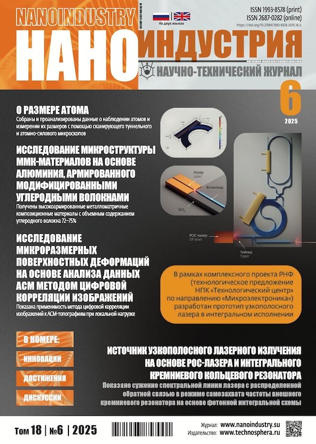
Источник узкополосного лазерного излучения на основе рос-лазера и интегрального кремниевого кольцевого резонатора
Аннотация
В данной работе продемонстрировано сужение спектральной линии лазера с распределенной обратной связью 210 кГц до 150 Гц в режиме самозахвата частоты внешнего кремниевого резонатора на основе фотонной интегральной схемы, что открывает перспективы создания компактных узкополосных лазеров для генерации малошумных микроволновых сигналов.
356-365
Компактные источники терагерцевого излучения в диапазоне от 2 до 5 ТГц: от лабораторного образца до коммерческого продукта
Аннотация
Сотрудники лаборатории квантово-каскадных лазеров МФТИ и Отделения сверхвысокочастотной полупроводниковой электроники им. В.Г.Мокерова Центра перспективной микроэлектроники НИЦ "Курчатовский институт" работают над созданием компактного и простого в использовании терагерцевого (ТГц) источника лазерного излучения, не требующего использования криогенных жидкостей.
366-369
Наноматериалы
Исследование микроструктуры металломатричных композиционных материалов на основе алюминия, армированного модифицированными углеродными волокнами
Аннотация
В работе представлены результаты исследования по определению толщины металлических покрытий на углеродных волокнах и микроструктуры металломатричных композиционных материалов на основе алюминия, армированного модифицированными углеродными волокнами. В качестве модификатора для углеродных волокон выступали защитные покрытия из металлов, такие как никель и медь. Данные покрытия позволили осуществить пропитку углеродного волокна расплавом алюминия с применением жидкофазного метода и получить высокоармированные металломатричные композиционные материалы с объемным содержанием углеродного волокна 72–75%.
370-378
Моделирование физических характеристик металлических островковых наноструктур
Аннотация
Представлены результаты физического моделирования функциональных характеристик датчиков полей и сред на основе островковых наноструктур в зависимости от их размеров. Показаны преимущества применения кобальта и никеля для датчиков слабых магнитных полей и алюминия с поверхностным слоем оксида алюминия – для датчика газовой среды. Приведены результаты зависимостей физических параметров магнитного поля и туннельной проводимости в островковых слоях кобальта и алюминия, соответственно, от расстояний между островковыми наноструктурами.
380-390