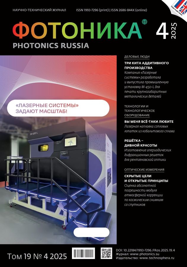
Stamp electron-beam nanolithography as a tool for fabricating aperiodic diffraction gratings for X-ray optics
- Authors: Arzhanov A.I.1,2, Shelkovnikov A.S.1, Shulga V.V.1, Aleksashin K.E.1, Kolesnikov A.O.1, Shatokhin A.N.1, Ragozin E.N.1, Naumov A.V.1,2
-
Affiliations:
- P. N. Lebedev Physical Institute of the Russian Academy of Sciences
- Moscow Pedagogical State University (MPGU)
- Issue: Vol 19, No 4 (2025)
- Pages: 292-295
- Section: Technologies & Technology Equipment
- URL: https://journals.eco-vector.com/1993-7296/article/view/686885
- DOI: https://doi.org/10.22184/1993-7296.FRos.2025.19.4.292.295
- ID: 686885
Cite item
Abstract
The results of fabrication and characterization of metallized aperiodic diffraction gratings (with a line density ranging from 150 to 570 lines per mm) using modernized scanning stamp electron-beam nanolithography machine ZBA-21 with a 200 nm process technological standard and a working area of up to 150 × 150 mm are presented. The characterization was performed using scanning atomic force microscopy.
Full Text
About the authors
A. I. Arzhanov
P. N. Lebedev Physical Institute of the Russian Academy of Sciences; Moscow Pedagogical State University (MPGU)
Email: a_v_naumov@mail.ru
ORCID iD: 0000-0001-9305-067X
Russian Federation, Moscow, Troitsk; Moscow
A. S. Shelkovnikov
P. N. Lebedev Physical Institute of the Russian Academy of Sciences
Email: a_v_naumov@mail.ruро
ORCID iD: 0000-0003-3391-2738
Russian Federation, Moscow, Troitsk
V. V. Shulga
P. N. Lebedev Physical Institute of the Russian Academy of Sciences
Email: a_v_naumov@mail.ru
Russian Federation, Moscow, Troitsk
K. E. Aleksashin
P. N. Lebedev Physical Institute of the Russian Academy of Sciences
Email: a_v_naumov@mail.ru
Russian Federation, Moscow, Troitsk
A. O. Kolesnikov
P. N. Lebedev Physical Institute of the Russian Academy of Sciences
Email: a_v_naumov@mail.ru
ORCID iD: 0000-0003-2511-762X
Russian Federation, Moscow, Troitsk
A. N. Shatokhin
P. N. Lebedev Physical Institute of the Russian Academy of Sciences
Email: a_v_naumov@mail.ru
ORCID iD: 0000-0002-6057-3535
Russian Federation, Moscow, Troitsk
E. N. Ragozin
P. N. Lebedev Physical Institute of the Russian Academy of Sciences
Email: a_v_naumov@mail.ru
ORCID iD: 0000-0001-5912-9229
Russian Federation, Moscow, Troitsk
A. V. Naumov
P. N. Lebedev Physical Institute of the Russian Academy of Sciences; Moscow Pedagogical State University (MPGU)
Author for correspondence.
Email: a_v_naumov@mail.ru
ORCID iD: 0000-0001-7938-9802
Russian Federation, Moscow, Troitsk; Moscow
References
- Soifer V. A. Diffractive nanophotonics and advanced information technologies. Herald of the Russian Academy of Sciences. 2014; 84(1):9–20. doi: 10.1134/S1019331614010067
- Eremchev I. Y., Prokopova D. V., Losevskii N. N., Mynzhasarov I. T., Kotova S. P., Naumov A. V. Three-dimensional fluorescence nanoscopy of single quantum emitters based on the optics of spiral light beams. Physics-Uspekhi. 2022;65(6):617–626. doi: 10.3367/UFNe.2021.05.038982
- Ragozin E. N., Vishnyakov E. A., Kolesnikov A. O., Pirozhkov A. S., Shatokhin A. N. Soft X-ray spectrometers based on aperiodic reflection gratings and their application. Physics-Uspekhi. 2021; 64 495–514. doi: 10.3367/UFNr.2020.06.038799
- Kovalets N. P., Kozhina E. P., Razumovskaya I. V., Arzhanov A. I., Naumov А. V. Scratching of metallized polymer films by vickers indenter as a method for controlled production of sers-active metasurfaces. Journal of Luminescence. 2024; 275:120803. doi: 10.1016/j.jlumin.2024.120803
- Vyalykh A. P., Skakunenko P. I., Shishova M. V., Semenko A. V., Afanasiev A. E., Belotelov G. S., Sutyrin D. V., Balykin V. I. Atom Chip and Diffraction Grating for the Laser Cooling of Ytterbium Atoms. JETP Letters, 119 (4), 285-293 (2024). doi: 10.1134/S0021364023604189.
- Kotova S. P., Losevsky N. N., Mayorova A. M., Samagin S. A. Optothermal traps based on sector diffraction optical elements. Bulletin of the Russian Academy of Sciences: Physics. 87 (12), 1767-1772 (2023). doi: 10.1134/s1062873823704038
- Kazakov I. A., Malakhov K. M., Kovalev E. E., Mkrtchyan A. A., Mishevsky M. S., Svetikov V. V., Shipulin A. V. Study of operational algorithm for interrogator with arrayed waveguide grating on a photonic integrated circuit. Photonics Russia 18 (2) 122-135 (2024). doi: 10.22184/1993-7296.FRos.2024.18.2.122.135
Supplementary files


